Customers Who Bought This Item Also Bought
overview
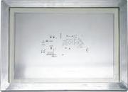
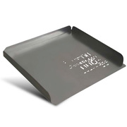
Multi-Level Stencils also known as step stencils are the solution for the new electronic assemblies which include mixed technology applications like fine pitch technology with through-hole and SMT technologies. This mix requires different amounts of solder paste for different parts.
Multi-Level Stencils can provide additional paste height in selected areas of the PCB (step-up) or reduced height deposits in other areas (step-down) in a specific section of the board.
SOME OF THE BIGGEST PROBLEMS THAT MULTI-LEVEL STENCILS
- Step Up Stencil for Through-Hole Intrusive Reflow: A trend has emerged to reflow through-hole components, instead of using wave soldering, along with the SMT components.
- Step Up Stencil for Ceramic BGA’s: Since the high melting temperature prevents the solder balls from melting at normal reflow temperatures, any slight coplanarity problem can result in an open contact to the CBGA balls.
- Multi-Level Stencil for Two-Print Operation for Mixed Technology: Consider a PCB that has a fully-populated pin grid array (PGA). Overprint (oversized aperture for the through-hole)is limited because of the fully-populated geometry.
- Bar code on the PCB: Many PCBs have bar code identifiers attached to the board surface. If it gets too close to board pads it can prevent the stencil from gasketing to these pads during printing. A simple solution is to use a stencil that has a relief pocket etched in the area of the bar code.
Step-up areas
Used to increase the volume and height of the solder deposit. Useful for ‘pin in paste’ and large format devices with co planarity consistency problems.
Step-down areas
Used to reduce the volume and height of the paste deposit (or possibly increase the volume depending on aperture area ratio and transfer efficiency). Useful to improve Deposit Volume Repeatability in fine line and micro package attachment.
"Stepless" steps
Ramped step-up areas, produced by the electroforming process, to increase paste deposits in selected areas of the stencil for large components or large features such as antenna’s or shieldings. Formed on the PCB side of the stencil to provide a smooth print surface for enclosed printheads etc while minimising smearing.
Step-relief cavities
Used to overcome board surface irregularities such as raised pads, vias, legends such as bar codes and edge clamping issues. These features also afford relief for paste print deposits in two step stencil printing processes… where the use of a thin stencil is followed up by a thicker stencil in order to achieve multi height deposits without the need for "keep out areas".
specs
| Technology | 100% laser cut |
| Material Used | Stainless Steel |
| Stencil Thickness | .002 - .016 inches |
| Minimum Cut Width | .002 inches |
| Maximum Size | 29"x29" inches |
| Aperture Tolerance | within .00025 inches |
| Allow for Fiducial Data | Yes |
| Allow for Panelized Data | Yes |

